Materials-to-Devices
Characterization/Development Service
Experts in computational material science, device reliability characterization, and
failure analysis, we are ready to bring all our knowledge and expertise to your project.
Contact us at: info@m2dsolutions.com.
Ensuring Success in Your Timeline
Market timing is integral to the success of any product, and we understand how critical this is to our clients' success. Our approach distinguishes itself by delivering accurate and meaningful solutions to highly specialized problems. Our deep understanding of the complex physics behind device properties enables us to deliver direct, tailored answers and practical solutions to our customers. We can provide an expedited and streamlined process for developing and/or qualifying devices through our highly effective, customized test measurements with controlled durations down to circuitry operation frequencies (sub-ns).
Methodology
Materials-to-Devices provides a specialized approach to wafer-level reliability testing
and analysis: Device Optimization via Materials Characterization™ (DOMaC). This technique
combines unique electrical test capabilities with world-class materials modeling and
simulations to solve challenging problems in device fabrication and evaluation.
Device evaluation is a complex endeavor driven by the necessity to answer key questions:
- Will the device perform as desired under circuity-relevant use conditions?
- What is the root cause of degradation and how can it be addressed?
A typical development process involves a sequence of fabrication, testing, modified fabrication, and subsequent retesting.
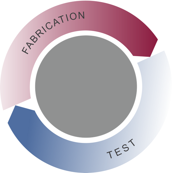
The traditional process is an ongoing fabrication-to-test loop that proceeds until the desired results are achieved. This is inefficient (slow and costly) for constructing complex structures of overlapping, interacting ultrathin layers having desirable electrical characteristics.
With predictive DOMaC the interrelationships between materials, physical processes, and electrical data can be evaluated simultaneously to identify degradation root causes and optimize fabrication decision-making.
What DOMaC Provides
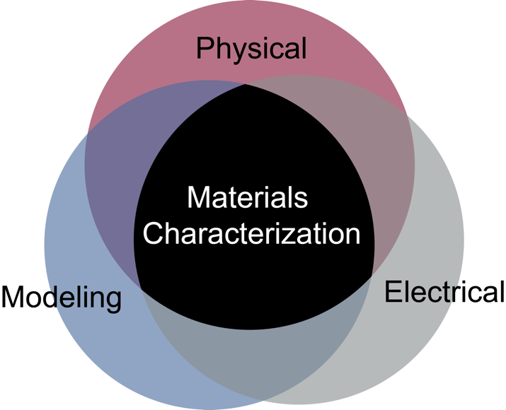
The Device Optimization via Materials Characterization approach utilizes a predictive physics-based analysis methodology, which combines physical, electrical, and modeling methods to deliver relevant comprehensive answers. This approach identifies the complex inherent material features and physical processes affecting electrical test data and provides a reliable assessment of device performance over time. Additionally, DOMaC furnishes insights into specific use conditions that extend the device's lifetime. It not only enables relevant and expedient evaluation but can inform pathways for device/system fabrication improvements.
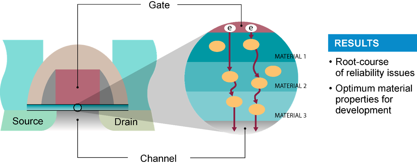
Schematic of the electron transport via defects in the multilayer transistor gate stack.
Materials Characterization benefits include:
- Furnishing performance and reliability evaluation under application-specific use conditions
- Establishing a range of use conditions that can extend a device's lifetime
- Assessing novel technologies ahead of product fabrication, providing feedback to fabrication
Technical Leadership Team
Dr. Gennadi Bersuker

Expert in electrical characterization and reliability, with more than 450 papers
Dr. David Gao

Expert in resistance switching, Catalysis, Lubrication, Multi-Scale Modeling, and Machine Learning, with more than 30 publications
Prof. Alex Shluger

Expert in theoretical methods for defects and processes in solids and interfaces, with more than 400 publications
Dr. Dmitry Veksler

Expert in device modeling and characterization, defect metrology, and failure analysis, with more than 150 publications